
HDI PCB/PCBA Solutions
ABIS helps hardware teams convert complex layout requirements into reliable, highly manufacturable HDI boards. Providing seamless supply chain coordination from quick-turn prototype validation to stable series production.Contact Now!
HDI PCB for Compact Electronics
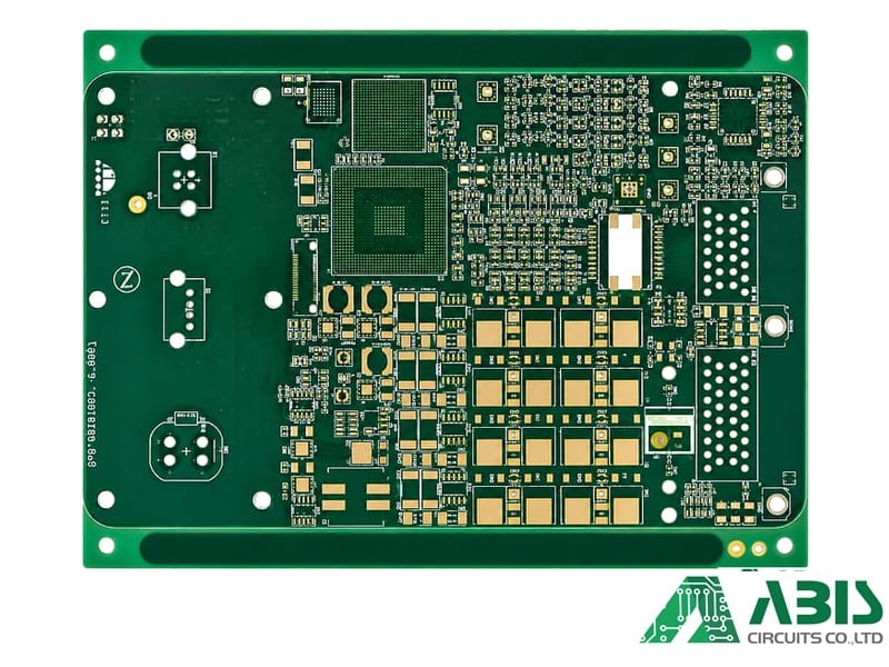
1+N+1 HDI PCB
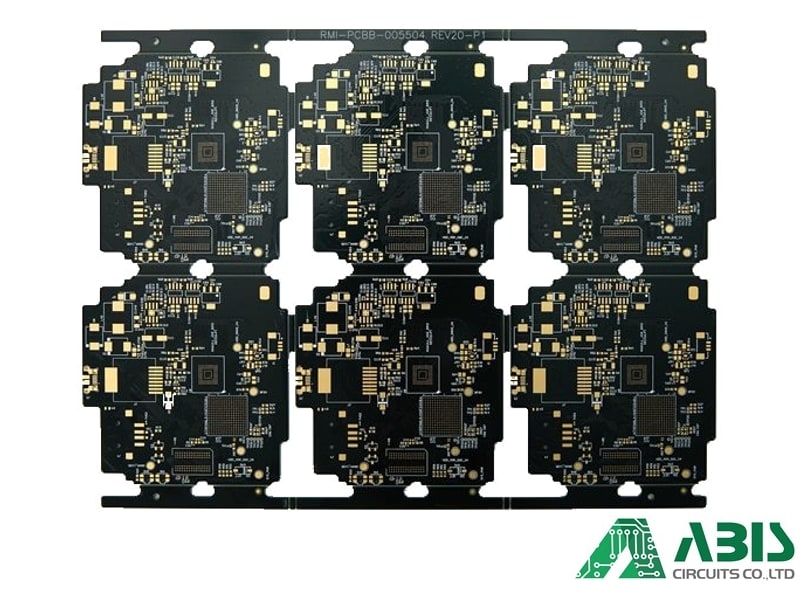
2+N+2 HDI PCB
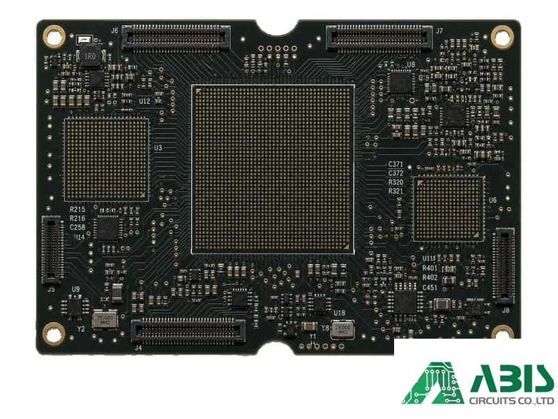
3+N+3 HDI PCB
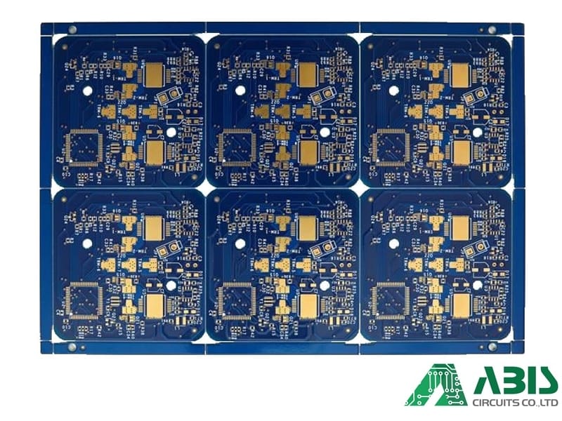
Microvia HDI PCB
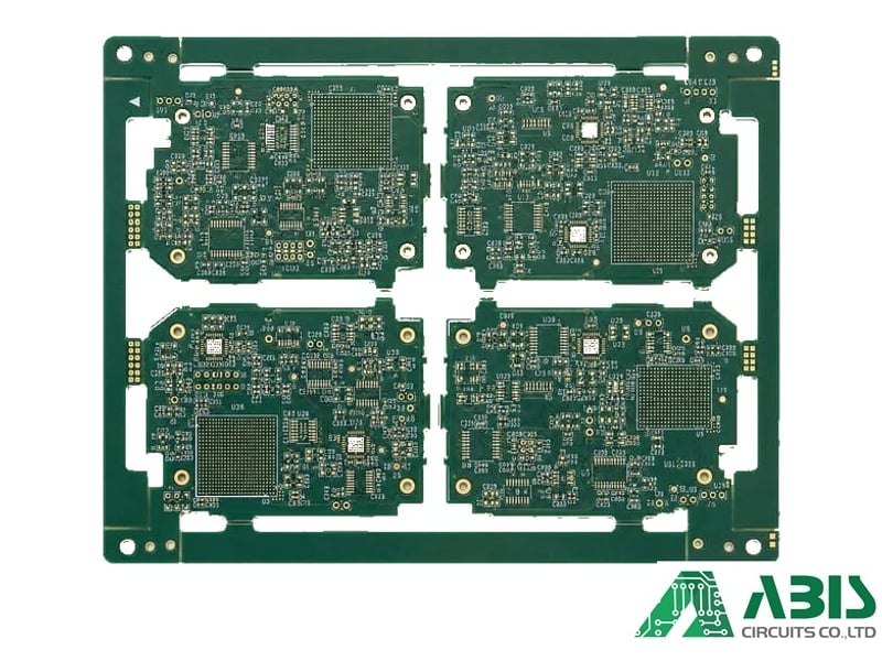
Stacked Microvia HDI PCB
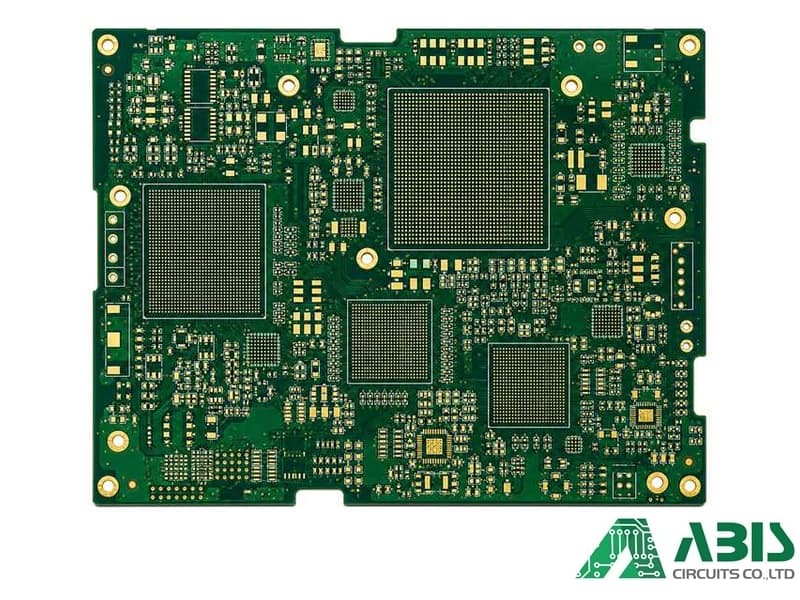
Staggered Microvia HDI PCB
Start Your HDI PCB Project
HDI PCB Support for Compact Electronics
We help electronics brands, hardware teams, and procurement managers reduce HDI production uncertainty through pro-active engineering file reviews, material validation, structure coordination, and full assembly integration.
Advanced Structural DFM Review
We provide rigorous DFM analysis on laser microvias, blind/buried vias, and fine-line spacing (down to 3/3mil), ensuring a clean signal path and flawless lamination.
Full-Scale OEM/ODM Project De-risking
We coordinate with elite tier-1 fabrication partners to convert your tight specs into a manufacturable solution, significantly reducing design and delivery risks.
PCB to Turnkey PCBA Integration
We coordinate HDI fabrication, complex component sourcing (ICs/BGAs), automated SMT assembly, and strict X-ray testing under one unified QA system, eliminating vendor handoff risks and costly shipping delays.
HDI PCB Application Coverage
HDI PCB projects for compact electronics where board space, routing density, fine-pitch components, and production reliability must be balanced.


A Practical PCB Partner for OEM/ODM Projects
Based in Shenzhen, we support customers who need more than basic PCB fabrication. With over 15 years of PCB and PCBA experience, we help engineering and purchasing teams reduce communication gaps, control production risks, and move projects from sample builds to series production and stable delivery.

What Our Customers Say About Our HDI PCB Manufacturing
OEM and ODM electronics teams choose us for reliable HDI PCB fabrication, responsive engineering support, and the ability to support projects from prototype to PCBA production.
The HDI PCB samples were delivered with stable quality and clear communication throughout the engineering review. Their team helped us confirm manufacturability before moving to production.

We needed compact PCBs for a high-density electronic device, and the team supported both PCB fabrication and PCBA assembly. The response was professional and the process was easy to manage.

Their HDI PCB manufacturing capability helped us handle fine routing, microvia requirements, and consistent production quality. It is a reliable option for long-term OEM projects.

How to Start Your HDI PCB Project
From engineering file review to PCB fabrication and optional PCBA assembly, we provide a clear and efficient cooperation process for OEM and ODM electronics projects.
01
02
03
Frequently asked questions
Yes. We provide complete turnkey HDI PCBA services, specifically capable of handling fine-pitch BGAs, using advanced automated SMT lines and 3D automated optical inspection.
Our strategic network supports certified copper-filled microvias (Via-in-Pad) and resin plugging with copper capping, ensuring excellent thermal management and flat pads for SMT soldering.
We implement mandatory automated X-ray inspection (AXI) for all HDI boards with BGA and QFN components to guarantee 100% solder joint integrity and detect internal voids.
Yes. We support HDI PCB prototype production, small-batch manufacturing, and volume production. Our team can help review your design before production and support project scaling from sample validation to stable batch delivery.
Yes. Our engineering team reviews your layer requirements and provides optimized HDI stack-up consultation to ensure signal integrity, controlled impedance, and balanced mechanical structures.
No. We support engineering teams with no strict MOQ, managing everything from quick-turn HDI prototype validation to high-volume series production runs.
We source high-performance, low-loss materials from trusted global brands to meet strict impedance and thermal demands.
Our production partners utilize high-precision LDI (Laser Direct Imaging) and advanced automated optical alignment systems to guarantee exact registration across complex multi-layer structures.
Absolutely. We sign strict Non-Disclosure Agreements (NDAs) to secure your proprietary Gerber files, ODB++ data, and BOM lists prior to any technical evaluation.
Please submit your complete Gerber files (or ODB++), custom stack-up drawings, complete BOM list with manufacturer part numbers, and estimated quantities.
