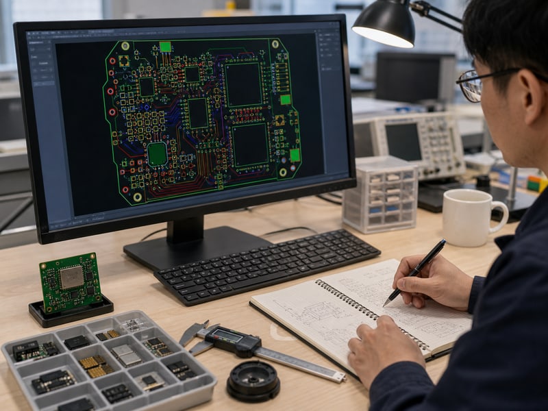
DFM Screening
Reduces sample failure, layout rework, and batch scrap caused by unchecked Gerber files, BOM issues, RF clearance conflicts, or assembly notes.

IoT and wireless products often face limited board space, unstable RF performance, battery-life pressure, and enclosure assembly constraints.

For smart locks, controllers, alarms, and home automation devices, reducing risks from wireless signal interference.

For wearable products, reducing risks related to limited space, lightweight structure, battery layout, and assembly tolerance.
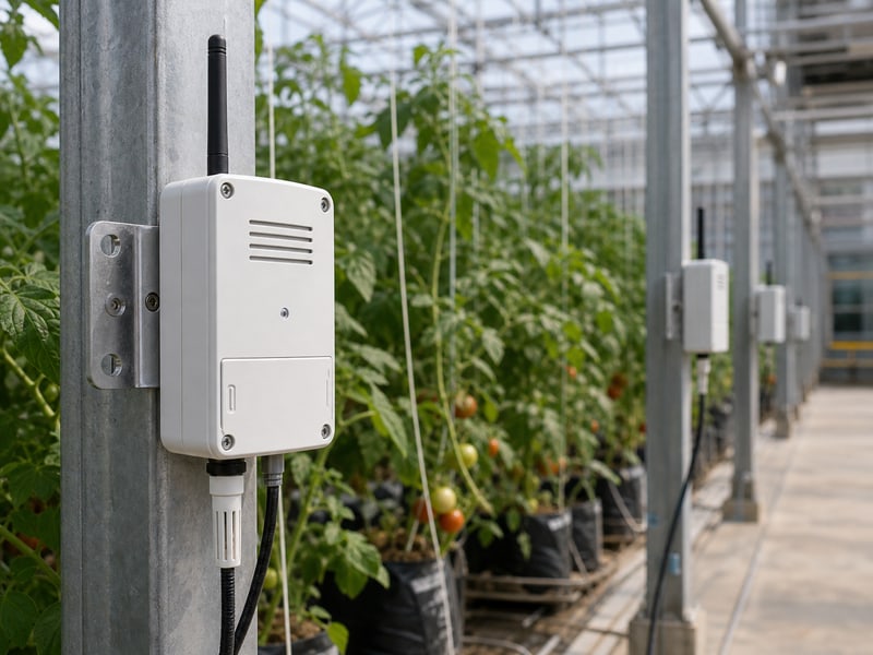
For wireless sensors, reducing risks from signal noise, unstable data transmission, compact routing, and long-term device operation.
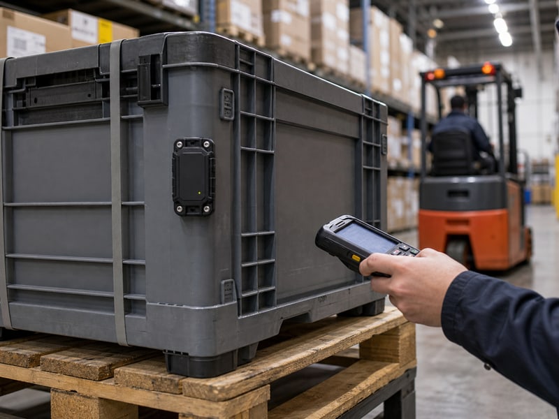
For GPS, Bluetooth, and wireless tracking products, reducing risks from antenna layout, power consumption, module integration.
Reduces sample failure, layout rework, and batch scrap caused by unchecked Gerber files, BOM issues, RF clearance conflicts, or assembly notes.
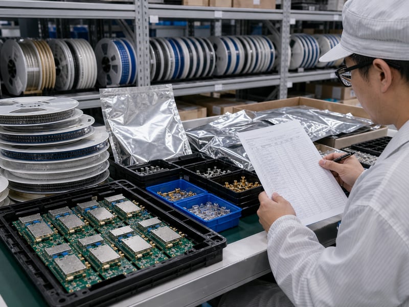
Reduces counterfeit, shortage, and substitution risks for MCU, sensor, RF module, connector, and power management components.
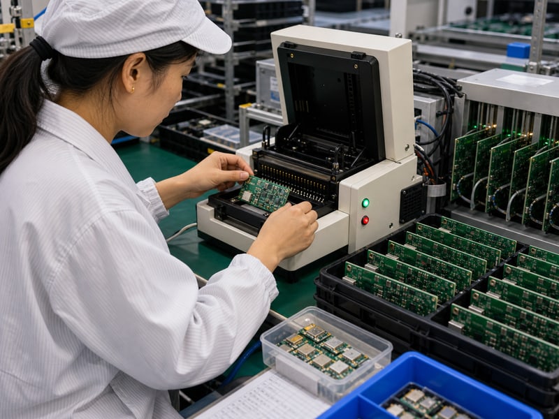
Reduces vendor friction, MOQ pressure, and production inconsistency from prototype validation to mixed-volume OEM/ODM manufacturing.
IoT and wireless device customers choose ABIS for compact PCB production, clear engineering review, and reliable quality from samples to repeat orders.
“ABIS reviewed our compact PCB design before production and pointed out several details that could affect assembly. The sample stage moved much smoother.”

“Our wireless sensor boards required stable quality across repeat orders. ABIS kept communication clear and production consistency easier to manage.”

“ABIS understood the space and RF concerns behind our tracking device PCB. Their review reduced risk before we moved to batch production.”

Based in Shenzhen, ABIS support customers who need more than basic PCB fabrication. With over 15 years of PCB and PCBA experience, we help engineering and purchasing teams reduce communication gaps, control production risks, and move projects from sample builds to series production and stable delivery.


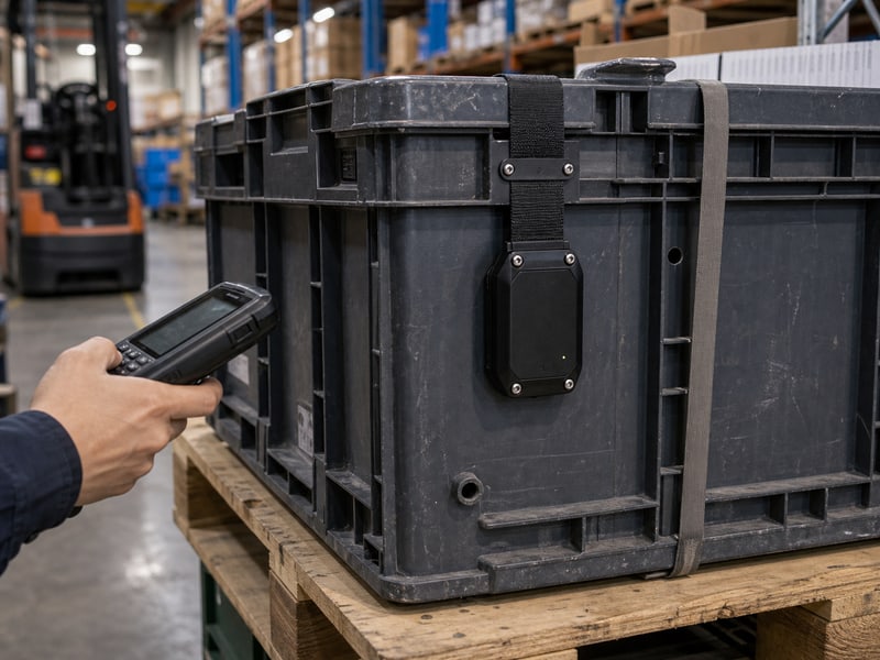

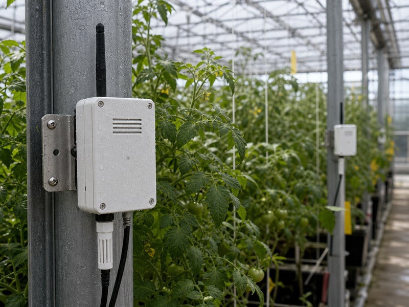
IoT and wireless devices often require HDI PCBs, multilayer PCBs, flexible PCBs, rigid-flex PCBs, thin PCBs, and PCBA assembly for compact layouts, antenna areas, batteries, and enclosure structures.
ABIS manufactures PCBs and PCBAs for smart home devices, wearable electronics, wireless sensors, Bluetooth devices, GPS trackers, smart meters, remote monitors, and connected consumer products.
Antenna clearance, RF routing, grounding, stack-up, board thickness, connector position, battery layout, surface finish, panelization, and enclosure tolerance should be reviewed before production.
Yes. ABIS can coordinate PCB fabrication, BOM review, component sourcing, SMT assembly, DIP assembly, inspection, and testing preparation, reducing friction from separate vendors.
ABIS reviews BOM details, confirms component specifications, checks availability, and coordinates sourcing channels before assembly to reduce incorrect parts, substitutions, shortages, and substandard components.ents.
Yes. ABIS can review Gerber files, BOM, stack-up, spacing, RF area, panelization, assembly notes, and production requirements before fabrication.
ABIS can arrange visual inspection, electrical testing, AOI, X-Ray inspection for selected assembly structures, and functional testing preparation according to project requirements.
Yes. ABIS can handle prototype, small-batch, pilot-run, and mixed-volume orders, making IoT production more practical before stable market demand.
ABIS confirms production schedules, delivery requirements, packaging details, and shipping options in advance to reduce delays from unclear timelines or shipment changes.
Yes. ABIS manages Gerber files, BOM data, and engineering documents with controlled internal access, and can provide RoHS, REACH, UL-related material or process documents when required.
