
High Frequency PCB & PCBA Sourcing Solutions
Reliable High Frequency PCB manufacturing and precision assembly services for RF, microwave, antenna, and advanced communication projects. Supporting low-loss materials, strict controlled impedance, and stable signal integrity.Contact Now!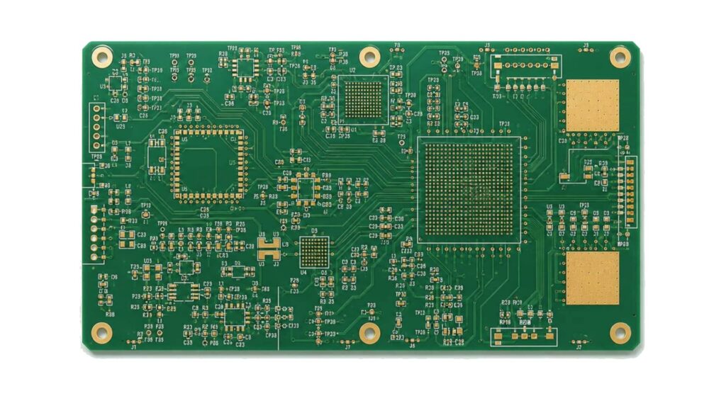
High Frequency PCB Options
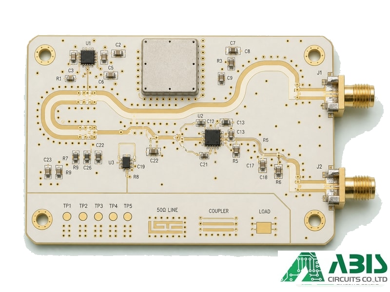
Rogers PCB
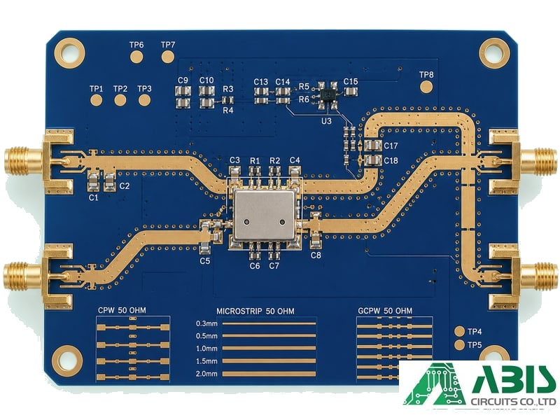
PTFE PCB
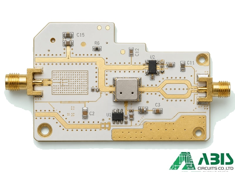
Ceramic PCB
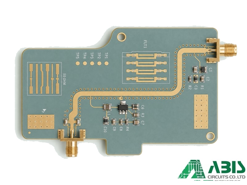
Taconic PCB
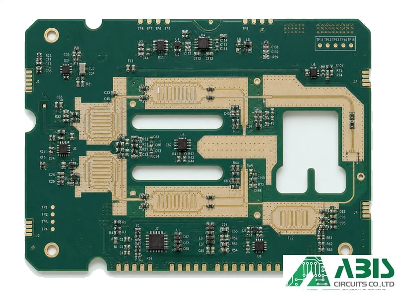
Hybrid High Frequency PCB
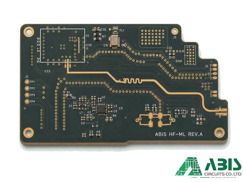
Multilayer High Frequency
Start Your High Frequency PCB Project
High Frequency PCB for Stability
For RF, microwave, and high-speed electronics, ABIS focuses on managing production factors that directly affect signal loss, impedance consistency, and raw material stability across the entire supply chain.
Signal Loss Control
100% low-loss materials and oversee controlled trace-geometry structures, drastically reducing signal attenuation and insertion loss concerns in RF, microwave, and antenna transmissions.
Impedance Stability
We enforce strict lamination tolerances, dielectric thickness controls, and copper etch consistency to maintain your target impedance within ±5% to ±10% tolerances.
Material Stability
We match your operating frequencies and SMT assembly environments with laminates featuring optimal Dk/Df consistency, low CTE, and superior thermal behavior to prevent delamination.
High Frequency PCB Applications
ABIS supports High Frequency PCB projects across signal-sensitive electronics where material performance, impedance control, and production consistency.


A Practical PCB Partner for OEM/ODM Projects
Based in Shenzhen, ABIS support customers who need more than basic PCB fabrication. With over 15 years of PCB and PCBA experience, we help engineering and purchasing teams reduce communication gaps, control production risks, and move projects from sample builds to series production and stable delivery.

What Business Partners Say
ABIS help clarify structure requirements, reduce assembly risks, and make it easier to move from prototype to production.
ABIS helped review our high frequency PCB stack-up and material requirements before production. Their communication helped us reduce design revisions, move project forward smoothly.

For our communication device project, ABIS supported controlled impedance PCB fabrication and assembly with stable quality. Their team understood the requirements and kept the process clear.

ABIS has been a reliable PCB partner for our high-speed signal boards. The sample verification and follow-up support also made repeat production easier to manage. We had a great cooperation.

How to Start Your High Frequency PCB Project
From engineering file review to PCB fabrication and optional PCBA assembly, we provide a clear and efficient cooperation process for OEM and ODM electronics projects.
01
02
03
Frequently asked questions
Through our specialized manufacturing network, we can achieve strict controlled impedance tolerances down to ±5% (standard is ±10%) based on your stack-up and trace geometry requirements.
Yes. We specialize in coordinating Hybrid High Frequency PCBs, choosing compatible bonding materials (PP) to manage thermal expansion differences and prevent delamination during SMT reflow.
Gerber files, stack-up, BOM, impedance requirements, material specifications, copper thickness, board thickness, surface finish, quantity, assembly details, and testing requirements help ABIS provide a more accurate quotation.
Every batch of controlled impedance boards undergoes mandatory TDR (Time Domain Reflectometry) testing. We provide full impedance coupon test reports along with the shipment.
We highly recommend ENIG (Electroless Nickel Immersion Gold) or Immersion Silver to ensure flat pads for fine-pitch components and to avoid skin-effect losses at high frequencies.
No. We support engineering teams with no strict MOQ constraints, managing everything from single-board RF prototype validation to small-to-medium series production.
Yes. We provide complete turnkey high-frequency assembly services, capable of handling high-speed ICs, specialized RF connectors, shields, and fine-pitch SMD components.
Absolutely. We protect your intellectual property. We sign strict NDAs before you share any proprietary Gerber files, layer stack-up drawings, or BOM lists.
Please provide your Gerber files (or ODB++), complete BOM list, material brand/series preference, specified layer stack-up with impedance targets, and quantities.
