With the rapid development of automotive electronics and power communication modules, ultra-thick copper foil circuit boards of 12oz and above have gradually become a kind of special PCB boards with broad market prospects, which have attracted more and more manufacturers’ attention and attention; With the wide application of
printed circuit boards in the electronic field, the functional requirements of equipment are getting higher and higher. Printed circuit boards will not only provide necessary electrical connections and mechanical support for electronic components, but also gradually be given more With additional functions, ultra-thick copper foil printed boards that can integrate power sources, provide high current and high reliability have gradually become popular products developed by the PCB industry and have broad prospects.
At present, research and development personnel in the industry have successfully developed a double-sided printed circuit board with a finished copper thickness of 10oz through the layered method of successive thickening of electroplated copper sinking + multiple solder mask printing assistance. However, there are few reports on the production of ultra-thick copper multilayer printed boards with a finished copper thickness of 12oz and above; this article mainly focuses on the feasibility study of the production process of 12oz ultra-thick copper multilayer printed boards. Thick copper step-by-step controlled deep etching technology + build-up lamination technology, effectively realizing the processing and production of 12oz ultra-thick copper multilayer printed boards.
Manufacturing process
2.1 Stack up design
This is a 4 layer, Outer/inner cooper thicknesss 12 oz,min width/space 20/20mil,stack up as below:

2.1 Analysis of processing difficulties
❶ Ultra-thick copper etching technology (copper foil is ultra-thick, difficult to etch): purchase special 12OZ copper foil material, adopt positive and negative controlled deep etching technology to realize the etching of ultra-thick copper circuits.
❷ Ultra-thick copper lamination technology: The technology of single-sided circuit-controlled deep etching by vacuum pressing and filling is used to effectively reduce the difficulty of pressing. At the same time, it assists the pressing of silicone pad + epoxy pad to solve the problem of ultra-thick copper laminate Technical problems such as white spots and lamination.
❸ The precision control of the two alignments of the same layer of lines: measurement of expansion and contraction after lamination, adjustment of the expansion and contraction compensation of the line; at the same time, the line production uses LDI laser direct imaging to ensure the overlap accuracy of the two graphics.
❹ Ultra-thick copper drilling technology: By optimizing the rotation speed, feed speed, retreat speed, drill life, etc., to ensure good drilling quality.
2.3 Process flow (take 4-layer board as an example)

2.4 Process
Due to the ultra-thick copper foil, there is no 12oz thick copper core board in the industry. If the core board is directly thickened to 12oz, the circuit etching is very difficult, and the etching quality is difficult to guarantee; at the same time, the difficulty of pressing the circuit after one-time molding is also greatly increased. , Facing a larger technical bottleneck.
In order to solve the above problems, in this ultra-thick copper processing, the special 12oz copper foil material is directly purchased during the structural design. The circuit adopts a step-by-step controlled deep etching technology, that is, the copper foil is first etched 1/2 thickness on the reverse side → pressed to form a thick copper core Board → etching on the front to obtain the inner layer circuit pattern. Due to the step-by-step etching, the difficulty of etching is greatly reduced, and the difficulty of pressing is also reduced.
❶ Line file design
Two sets of files are designed for each layer of the circuit. The first negative file needs to be mirrored to ensure that the circuit is in the same position during the forward/reverse control deep etching, and there will be no misalignment.
❷ Reverse control deep etching of circuit graphics

❸ Secondary circuit graphics alignment accuracy control
In order to ensure the coincidence of the two lines, the expansion and contraction value should be measured after the first lamination, and the line expansion and contraction compensation should be adjusted; at the same time,
The automatic alignment of LDI laser imaging effectively improves the alignment accuracy. After optimization, the alignment accuracy can be controlled within 25um.

❹ Super thick copper etching quality control
In order to improve the etching quality of ultra-thick copper circuits, two methods of alkaline etching and acid etching were used for comparative testing. After verification, the acid-etched circuit has smaller burrs and higher line width accuracy, which can meet the etching requirements of ultra-thick copper. The effect is shown in Table 1.

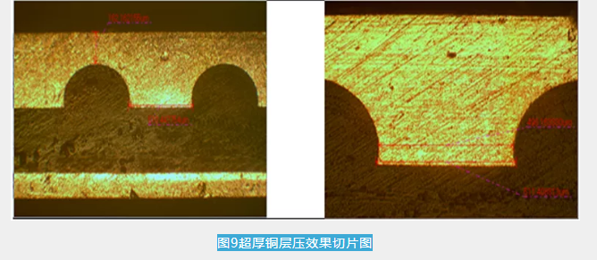
With the advantages of step-by-step controlled deep etching, although the difficulty of lamination has been greatly reduced, if the conventional method is used for lamination, it still faces many problems, and it is easy to produce hidden quality problems such as lamination white spots and lamination delamination. For this reason, after the process comparison test, the use of silicone pad pressing can reduce laminating white spots, but the board surface is uneven with the pattern distribution, which affects the appearance and the quality of the film; if the epoxy pad is also assisted, the pressing quality is significantly improved , Can meet the pressing requirements of ultra-thick copper.
❶ Super thick copper lamination method

❷ Super thick copper laminate quality

Judging from the condition of the laminated slices, the circuit is fully filled, without micro-slit bubbles, and the entire deep-etched part is deeply rooted in the resin; at the same time, due to the problem of ultra-thick copper side etching, the top line width is much larger than the narrowest line width in the middle At about 20um, this shape resembles an "inverted ladder", which will further enhance the grip of the pressing, which is a surprise.
❷ Ultra-thick copper build-up technology
Using the above-mentioned step-by-step controlled deep etching technology + lamination process, layers can be added successively to realize the processing and production of ultra-thick copper multi-layer printed boards; at the same time, when the outer layer is made, the copper thickness is only about approx. 6oz, in the range of the conventional solder mask process capability, greatly reduces the process difficulty of solder mask production and shortens the cycle of solder mask production.
Ultra-thick copper drilling parameters
After total pressing, the thickness of the finished plate is 3.0mm, and the overall copper thickness reaches 160um, which makes it difficult to drill. This time, in order to ensure the quality of the drilling, the drilling parameters were specially adjusted locally. After optimization, the slice analysis showed that the drilling has no defects such as nail heads and coarse holes, and the effect is good.


Summary
Through the process research and development of the ultra-thick copper multilayer printed board, the positive and negative controlled deep etching technology is used, and the silicone pad + epoxy pad is used to improve the quality of the lamination during lamination, which effectively solves the difficulty of etching the ultra-thick copper circuit Common technical problems in the industry, such as ultra-thick laminate white spots and multiple printing for solder mask, have successfully realized the processing and production of ultra-thick copper multilayer printed boards; its performance has been verified to be reliable, and it has satisfied customers' Special demand for current.
❶ Step-by-step control deep etching technology for positive and negative lines: effectively solve the problem of ultra-thick copper line etching;
❷ Positive and negative line alignment accuracy control technology: effectively improve the overlap accuracy of the two graphics;
❸ Ultra-thick copper build-up lamination technology: effectively realizes the processing and production of ultra-thick copper multilayer printed boards.
Conclusion
Ultra-thick copper printed boards are widely used in large-scale equipment power control modules due to their over-current conduction performance. Especially with the continuous development of more comprehensive functions, ultra-thick copper printed boards are bound to face wider Market prospects. This article is just for reference and reference for peers.

 Englishen


