10 characteristics of high reliability PCB,
1. 20μm hole wall copper thickness of Printed circuit board,
Benefits: Enhanced reliability, including improved z-axis expansion resistance.
Risks of not doing so: blow holes or outgassing, electrical connectivity issues during assembly (separation of inner layers, breakage of hole walls), or possible failure under load conditions in actual use.
2. No welding repair or open circuit repair
Benefit: Perfect circuit ensures reliability and safety, no maintenance, no risk.
Risk of not doing this: If repaired incorrectly, you will create an open circuit on the board. Even if repaired 'properly', there is a risk of failure under load conditions (vibration, etc.) that may fail in actual use.
3. Use international well-known CCL,
Benefits: Improved reliability, longevity and known performance.
Risks of not doing this: Using inferior quality sheets will greatly shorten the life of the product, and at the same time, poor mechanical properties of the sheet mean that the board will not perform as expected under the assembled conditions, for example: high expansion properties can lead to delamination, open circuit and warping buckling problems, and weakened electrical properties can result in poor impedance performance.
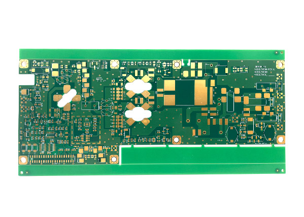
The materials of ABIS PCB factory are all from well-known domestic and foreign board suppliers, and have reached long-term strategic cooperative relations with suppliers to stabilize supply.
4. Use high-quality ink
Benefits: Ensure the quality of circuit board printing, improve the fidelity of image reproduction, and protect the circuit.
Risk of not doing so: Poor quality inks can cause adhesion, flux resistance and hardness problems. All of these problems can cause the solder mask to detach from the board and eventually lead to corrosion of the copper circuit. Poor insulation properties can cause short circuits due to accidental electrical continuity/arcing.
5. Exceed the cleanliness requirements of IPC specifications
Benefit: Improved PCB cleanliness improves reliability.
Risks of not doing this: Residues on the board, solder build-up can present a risk to the solder mask, ionic residue can cause corrosion of the solder surface and risk of contamination which can lead to reliability issues (bad solder joints/electrical failures), and Ultimately increasing the probability of actual failures.
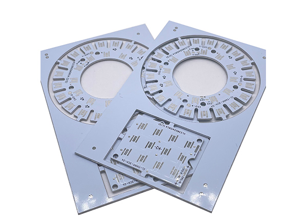
White solder mask Aluminum Circuit Board
6. Strictly control the service life of each surface treatment
Benefits: Solderability, reliability, and reduced risk of moisture intrusion.
Risks of not doing this: Solderability issues may occur due to metallographic changes in the surface finish of older boards, and moisture intrusion may cause delamination, inner layers and hole walls during assembly and/or actual use Separation (open circuit), etc. Taking the surface tin spraying process as an example, the thickness of tin spraying is ≧1.5μm, and the service life is longer.
7. High quality plug hole
Benefit: High-quality plug holes in the PCB factory will reduce the risk of failure during assembly.
Risk of not doing this: Chemical residues from the gold immersion process can remain in the holes that are not fully plugged, causing problems such as solderability. In addition, there may also be tin beads hidden in the holes. During assembly or actual use, the tin beads may splash out and cause a short circuit.
8. The tolerance of CCL meets the requirements of IPC 4101 ClassB/L
Benefit: Tight control of dielectric layer thickness reduces deviation from expected electrical performance.
Risk of not doing so: Electrical performance may not meet specified requirements, and components from the same batch may vary widely in output/performance.
9. Strictly control the tolerances of shapes, holes and other mechanical features
Benefit: Tightly controlled tolerances improve product dimensional quality - improved fit, form and function.
Risks of not doing this: Problems during assembly, such as alignment/mating (problems with press-fit pins are only discovered when assembly is complete). In addition, the mounting into the base can also be problematic due to increased dimensional deviations. According to high reliability standards, the hole position tolerance is less than or equal to 0.075mm, the hole diameter tolerance is PTH±0.075mm, and the shape tolerance is ±0.13mm.
10. The thickness of the solder mask is thick enough
Benefits: Improved electrical insulation properties, reduced risk of peeling or loss of adhesion, increased resistance to mechanical shock – wherever it occurs!
Risk of not doing so: Thin solder mask can cause adhesion, flux resistance and hardness problems. All of these problems can cause the solder mask to detach from the board and eventually lead to corrosion of the copper circuit. Poor insulation properties due to thin solder mask, can cause short circuits due to accidental conduction/arcing.
Others, please rfq, here!

 Englishen


